


An article on third-generation semiconductors
Time:2020.09.08
View:
The semiconductor industry has gone through three stages so far:
The first generation of semiconductor materials is represented by silicon;
The second-generation semiconductor material gallium arsenide has also been widely used;
The third-generation semiconductor materials represented by gallium nitride, silicon carbide, zinc oxide, aluminum oxide, and diamond.
Compared with the previous two generations of products, they have significant performance advantages. With their advantages of high efficiency, high density, and high reliability, they play an important role in the fields of new energy vehicles, communications and household appliances, and become the new focus of the industry.

1. Industry overview
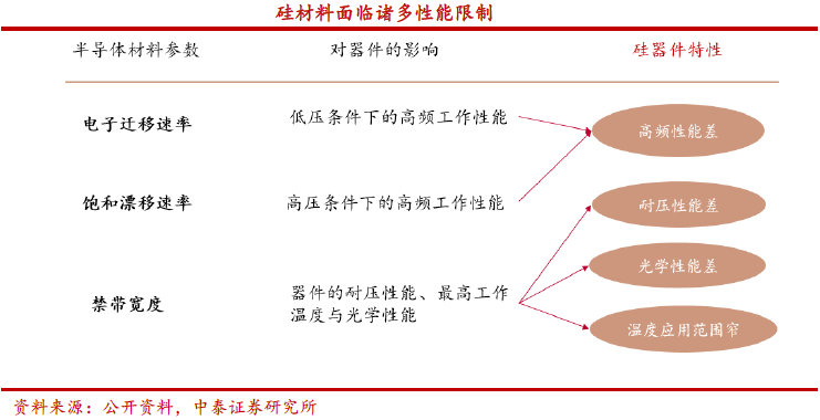
1.1 Limitations of semiconductor silicon (Si) materials
Since the 1950s, the first generation of semiconductor materials represented by silicon (Si) materials has triggered rapid development in the field of microelectronics with integrated circuits (IC) as the core. However, due to the narrow band gap, electron mobility and breakdown electric field of silicon materials, the application of Si in the field of optoelectronics and high-frequency and high-power devices is subject to many restrictions.
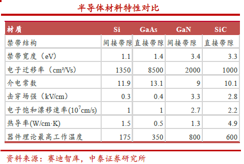
1.2 Performance comparison of semiconductor materials
As the bottleneck of Si materials has become increasingly prominent, the second-generation semiconductor materials represented by gallium arsenide (GaAs) have begun to emerge, making the application of semiconductor materials enter the field of optoelectronics, especially in infrared lasers and high-brightness red light diodes. . The rise of the third generation of semiconductor materials is based on the breakthrough of p-type doping of gallium nitride (GaN) materials, and is marked by the successful development of high-brightness blue light-emitting diodes (LED) and blue lasers (LD), including GaN , Silicon carbide (SiC) and zinc oxide (ZnO) and other wide band gap materials.
1.3 Application of third-generation semiconductor materials
The third-generation semiconductors (mainly SiC and GaN) are also known as wide-bandgap semiconductors. The band gap is above 2.2eV. It has high breakdown electric field, high saturated electron velocity, high thermal conductivity, high electron density, high mobility, etc. Features have gradually received attention. Compared with SiC and GaN, the former developed earlier than GaN and has a higher technological maturity; a big difference between the two is thermal conductivity, which makes SiC dominate in high-power applications; at the same time, due to GaN has a higher electron mobility, so it can have a higher switching speed than SiC or Si. In high-frequency applications, GaN has advantages.

2. Overview of SIC Industry
2.1 Overview of SiC industry
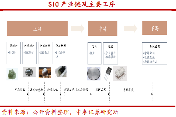
The SiC production process is divided into three major steps: SiC single crystal growth, epitaxial layer growth, and device manufacturing, which correspond to the three major links of the industry chain substrate, epitaxy, devices and modules.
Among them, SiC substrates are usually manufactured by the Lely method, and international mainstream products are transitioning from 4 inches to 6 inches, and 8-inch conductive substrate products have been developed.
SiC epitaxy is usually manufactured by chemical vapor deposition (CVD) method, and is divided into n-type and p-type epitaxial wafers according to different doping types.
In terms of SiC devices, 600~1700VSiC SBD and MOSFETs have been industrialized internationally. The withstand voltage level of mainstream products is below 1200V, and the packaging form is mainly TO packaging.
2.2 SiC industry structure
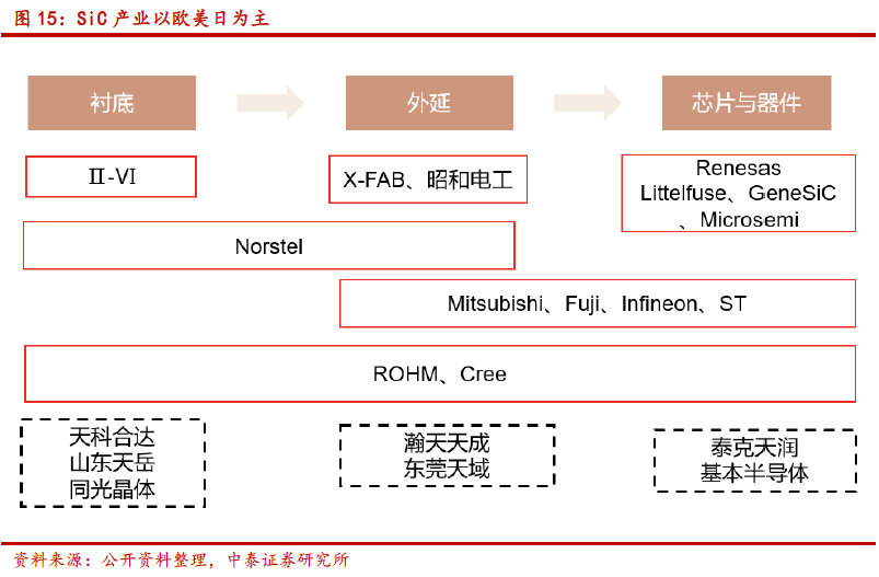
The global SiC industry structure presents a three-pronged situation of the United States, Europe, and Japan. Among them, the United States is the largest in the world. 70% to 80% of global SiC production comes from American companies. Typical companies are Cree and Ⅱ-VI; Europe has a complete SiC substrate, epitaxy, device and application industrial chain, and the typical company is Infineon , STMicroelectronics, etc.; Japan is a leader in equipment and module development. Typical companies are Rohm Semiconductor, Mitsubishi Electric, Fuji Electric, etc.
2.3 SiC power device market space
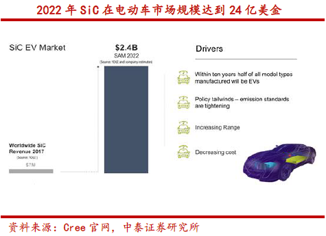
According to Yole’s forecast, the SiC power device market will grow at a compound annual growth rate of 31% from 2017 to 2023, and will exceed US$1.5 billion in 2023. Cree, the leader in the SiC industry, is more optimistic. SiC's market space for electric vehicles will quickly grow to US$2.4 billion, which is 342 times the overall revenue of automotive SiC (US$7 million) in 2017.
3. Overview of the GaN industry
3.1 GaN material characteristics
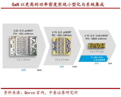
GaN materials have unique advantages over Si/SiC. Both GaN and SiC belong to the third generation of wide-bandgap semiconductor materials. Compared with SiC, which has been developed for more than ten years, GaN power devices are a latecomer. It has wide-bandgap materials with similar performance advantages to SiC, but has a greater cost. Control potential. Compared with traditional Si materials, power devices based on GaN materials have higher power density output and higher energy conversion efficiency, and can make the system smaller and lighter, effectively reducing the volume and weight of power electronic devices. Thereby greatly reducing system production and production costs.
3.2 Development of GaN devices
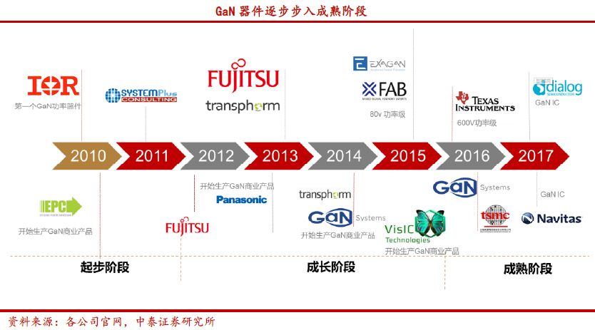
GaN-based LEDs began to shine in the 1990s and are now the mainstream of LEDs. Since the beginning of the 20th century, GaN power devices have been gradually commercialized. In 2010, the first GaN power device was put on the market by IR. After 2014, 600V GaN HEMT has become the mainstream of GaN devices. In 2014, the industry grew GaN devices on 8-inch SiC for the first time.
3.3 GaN application scenarios
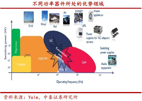
GaN, SiC, and Si materials each have their own advantages, but there are also overlaps. GaN material has the highest electronic saturation drift rate and is suitable for high-frequency application scenarios, but it is inferior to SiC in high-voltage and high-power scenarios. As the cost drops, GaN is expected to replace silicon-based power devices such as diodes, IGBTs, and MOSFETs in the low- and medium-power fields. In terms of voltage, 0~300V is the advantage of Si materials, above 600V is the advantage of SiC, and between 300V and 600V is the advantage of GaN materials.
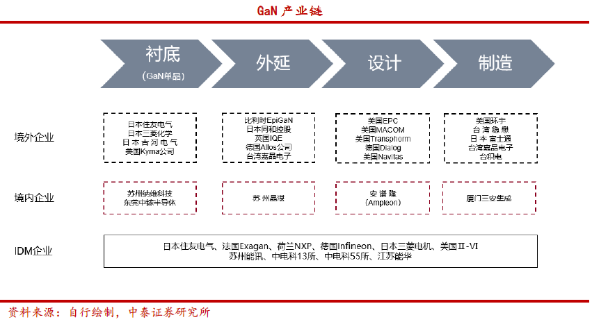
3.4 Overview of GaN Industry Chain
GaN is similar to the SiC industry chain. The links in the GaN device industry chain are: GaN single crystal substrate (or SiC, sapphire, Si) → GaN material epitaxy → device design → device manufacturing. The current industry is dominated by IDM companies, but the division of labor has begun to appear in the design and manufacturing links. For example, the traditional silicon wafer foundry TSMC has begun to provide GaN process foundry services, and domestic Sanan Integration also has mature GaN process foundry services. From the perspective of related companies in all aspects, European and American companies are basically the main ones, and Chinese companies have already set foot.
Author: Kepler Industrial Research Institute