


17 kinds of components PCB packaging illustration book, full of beauty!
Time:2020.09.08
View:


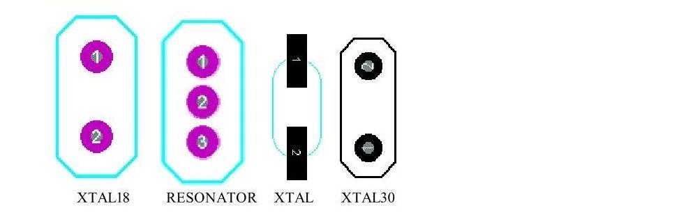
Crystal oscillator
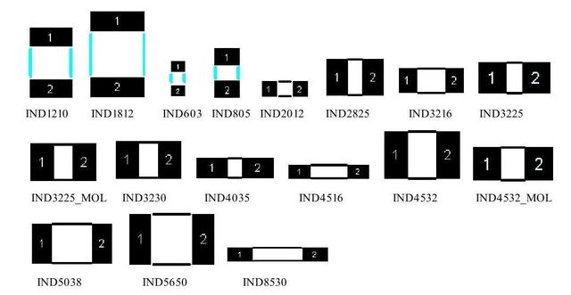
inductance
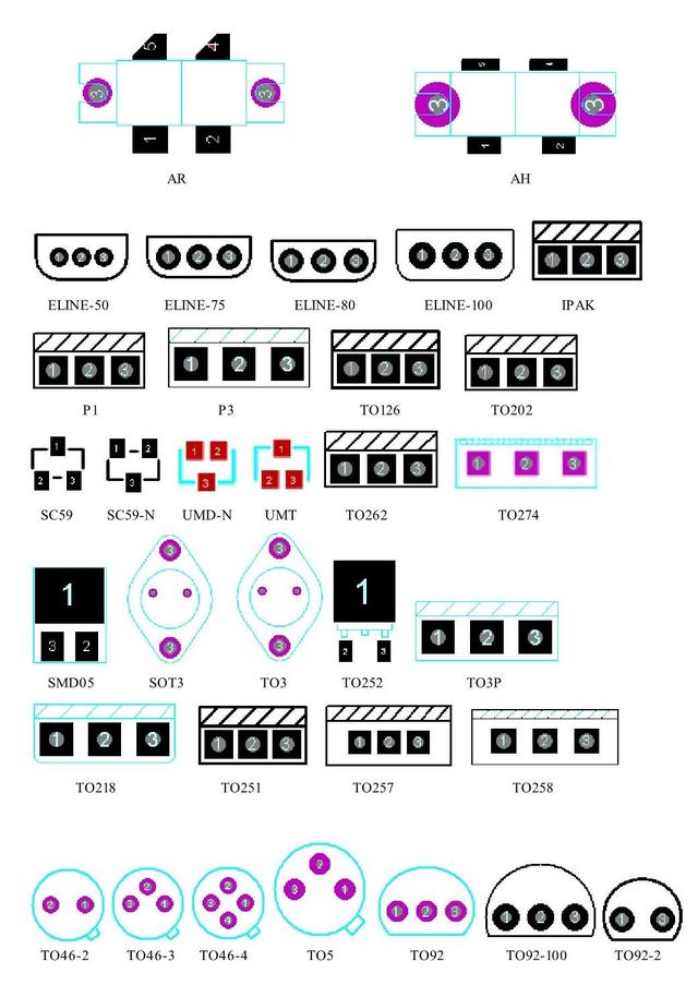
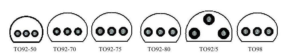
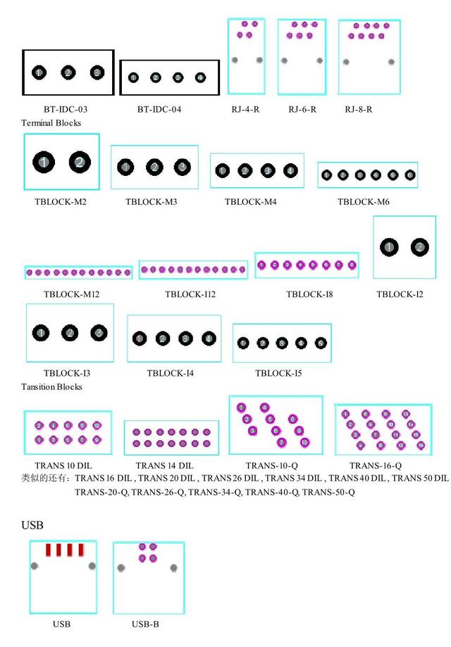
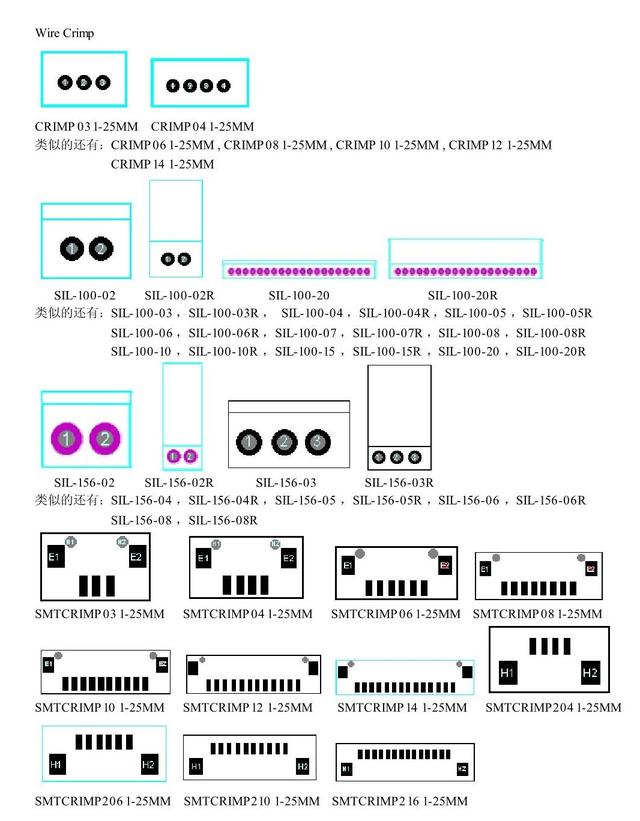
Connector


Discrete Components


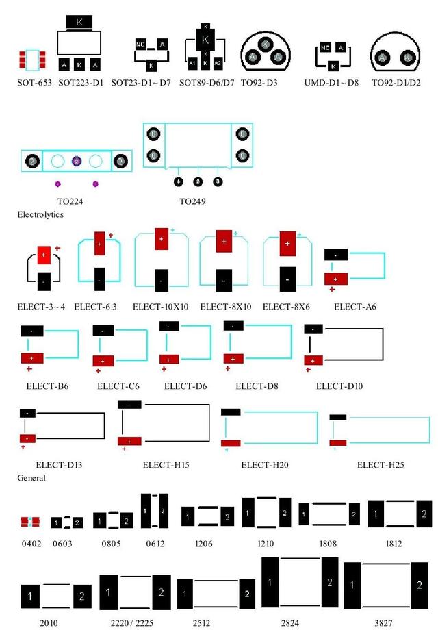
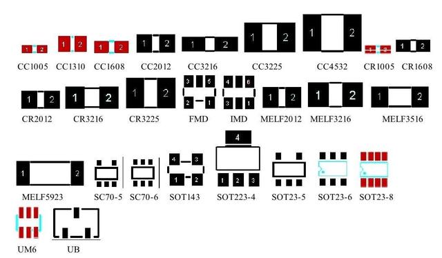
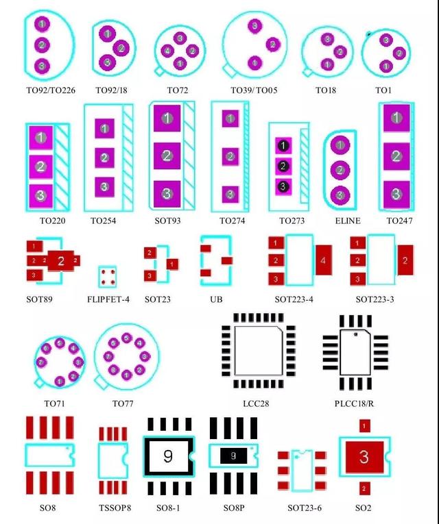
Transistor
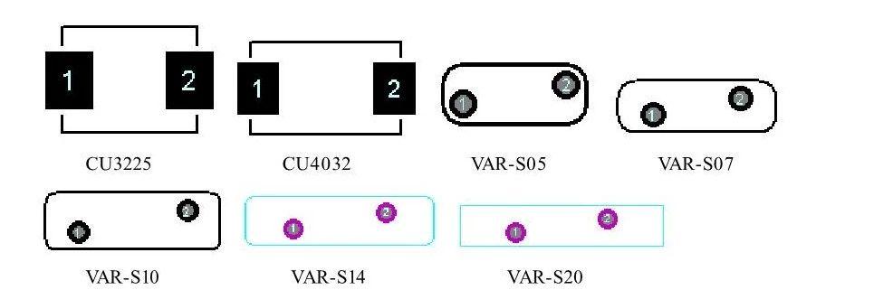
Variable capacitance
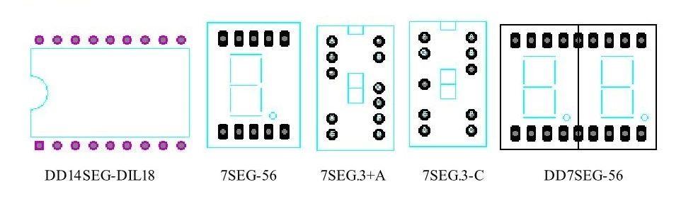
Digital Tube

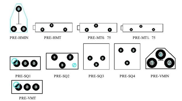
Adjustable resistance
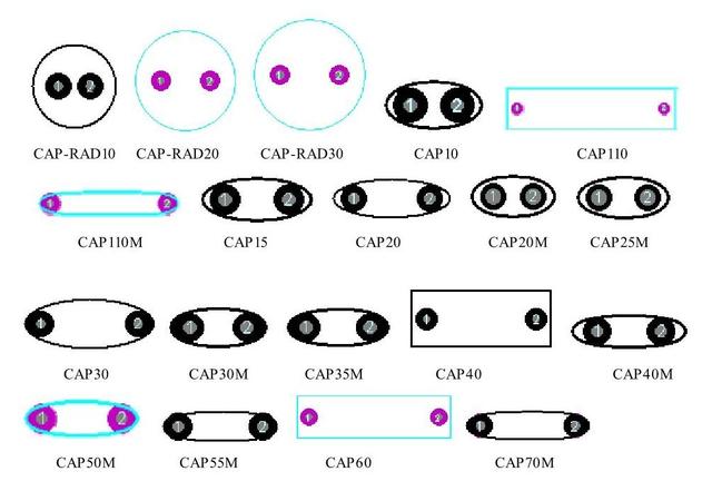
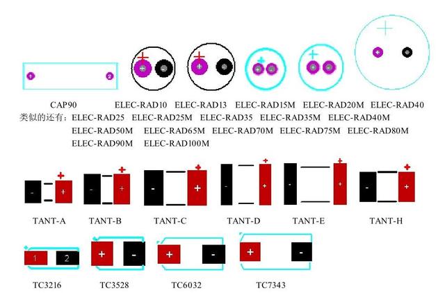
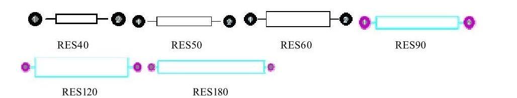
resistance
Exclusion

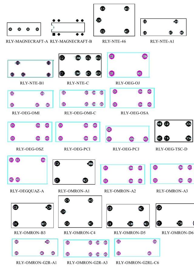
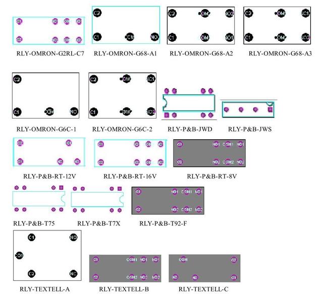
Relay
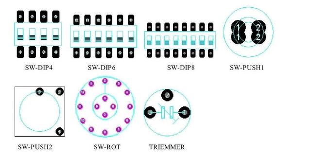
switch
Jumper

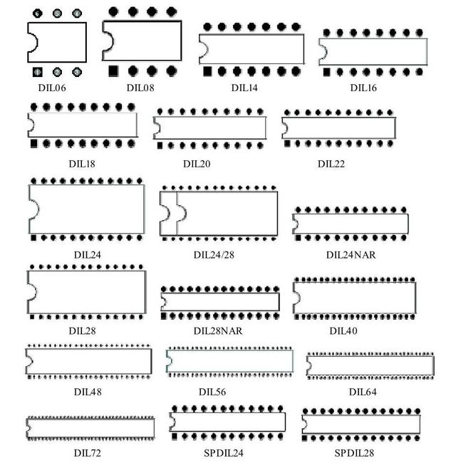
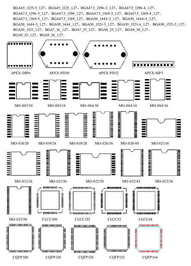
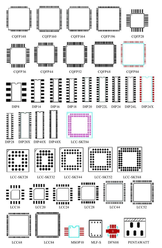
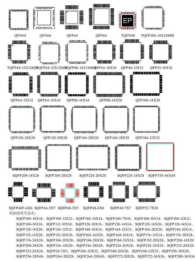
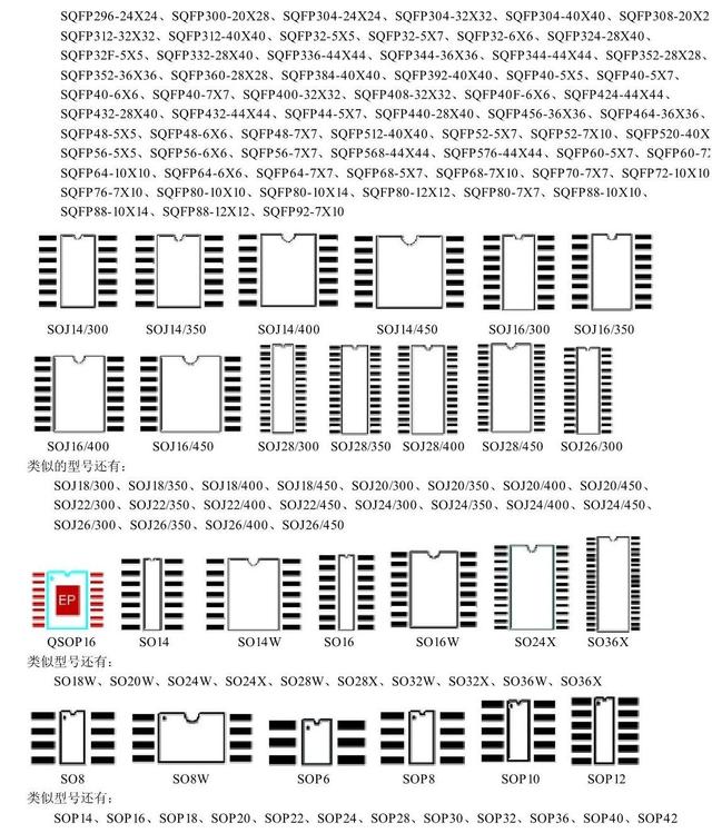
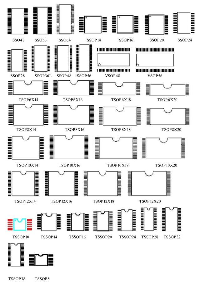
integrated circuit
1.5mmBGA
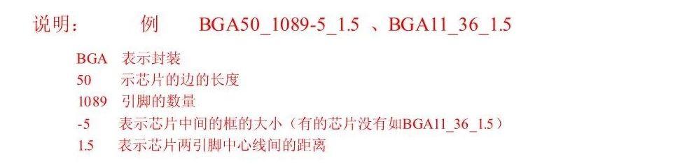

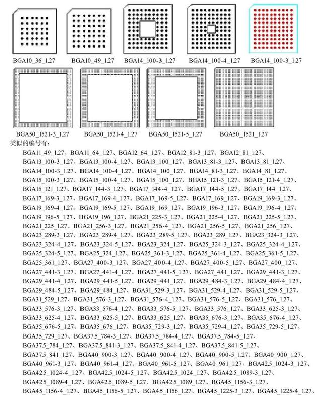
1mmBGA
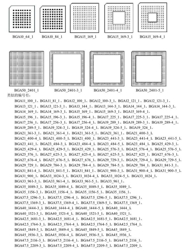

1.27BGA
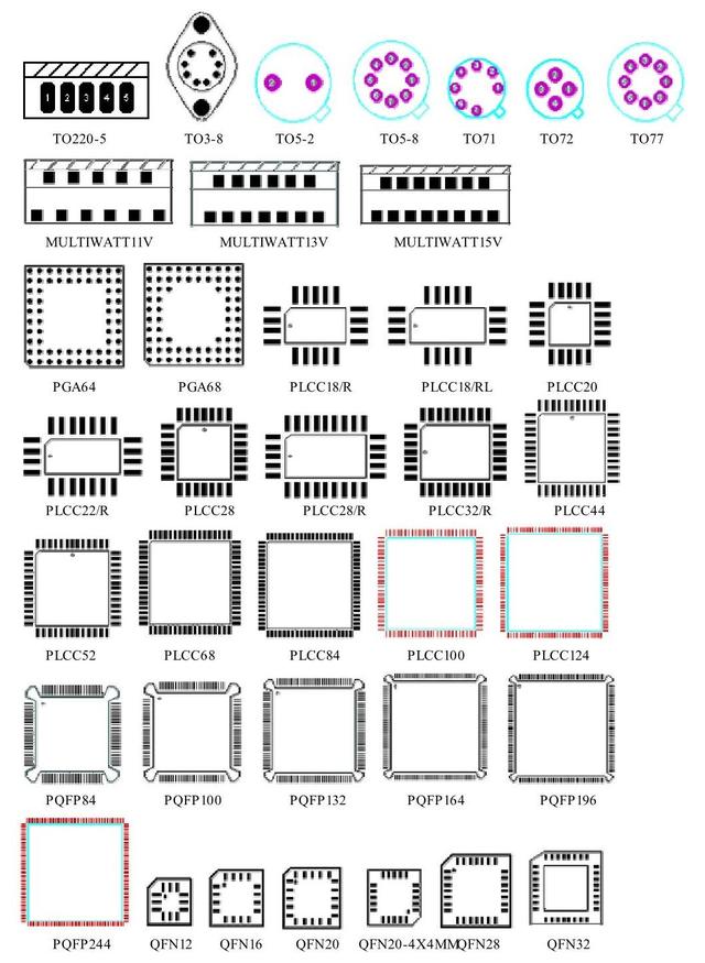
A well-qualified device package should meet the following conditions:
1. The designed pad should be able to meet the size requirements of the length, width and spacing of the target device pin.
Special attention should be paid to: the dimensional error produced by the device pin itself should be taken into account in the design --- especially the precise and detailed devices and connectors.
Otherwise, it may lead to different batches of the same type of devices, sometimes the welding process yield is high, sometimes large production quality problems occur!
Therefore, the compatibility design of the pad (appropriate and common to most large manufacturers' device pad size design) is very important!
On this point, the simplest requirements and inspection methods are:
Put the actual target device on the pad of the PCB board for observation, if each pin of the device is in the corresponding pad area.
The package design of this pad is basically not a big problem. Conversely, if some of the pins are not in the pad, it is not good.
2. The designed pad should have an obvious direction mark, preferably a universal and easily distinguishable direction polarity mark. Otherwise, when there is no qualified PCBA sample for reference,
If a third party (SMT factory or private outsourcing) does the welding process, the problem of reverse polarity and wrong welding will easily occur!
3. The designed pad should be able to meet the processing parameters, requirements and processes of the specific PCB circuit factory itself.
For example, the pad line size, line spacing, character length and width that can be designed, etc. If the PCB size is large, it is recommended that you design according to the popular and common PCB factory process in the market, so that when the PCB supplier is changed due to quality or business cooperation issues, there are too few PCB manufacturers to choose from and the production schedule is delayed.
This article is organized from the Internet.
泰科天润官网:http://www.globalpowertech.cn/